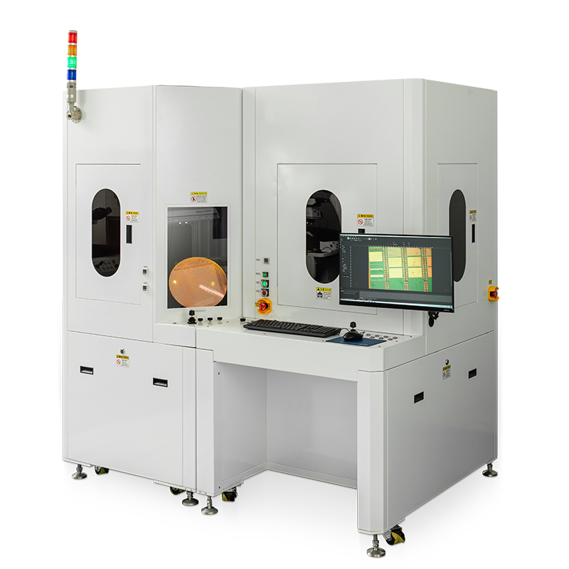
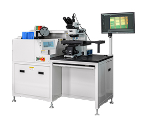
BAWL-12AS Automatic Focusing Wafer Inspection System
Introduction
The BAWL-12AS features and excellent optical imaging system, enabling high-definition capture of micro details on wafers. With a versatile macro inspection module and a flexible and easy-to-use remote-control joystick, it enables multi-angle, full-field macro inspection, making it an efficient tool for wafer defect analysis.
Details
Overview
Packaging & Delivery:
Packaging Details:Strong Carton with Polyfoam Protection
Port:Beijing
Lead Time:Within 2-4 Weeks after Receiving Payment
Introduction
Equipped with a fully automated wafer handling system, achieving efficient macro/micro inspection. The BAWL-12AS features and excellent optical imaging system, enabling high-definition capture of micro details on wafers. With a versatile macro inspection module and a flexible and easy-to-use remote-control joystick, it enables multi-angle, full-field macro inspection, making it an efficient tool for wafer defect analysis. BAWL-12AS provide leading semiconductor process optical inspection solutions.
Feature
1.EFEM system
The EFEM system is equipped with automatic loading and unloading modules and is compatible with various wafer sizes. It is an essential component of wafer inspection equipment. In a highly clean environment, individual wafers are transferred to the inspection module through a precision mechanical arm. The core components include the loadport, wafer transport robot, and wafer aligner.
The advanced loadport can open and close FOUP lids, and it can also be equipped with barcode scanners and RFID reading functions. The efficient recognition system can quickly and accurately identify different wafer cassette types, such as FOUP, FOSB, and Open Cassette.
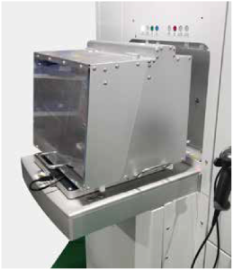
8 inch Open Cassette
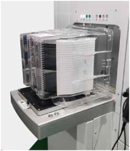
12 inch FOSB
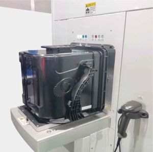
12 inch FOUP
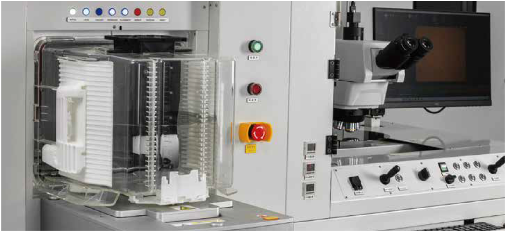
2.Mapping
Using a high-precision optical detection system, wafers are scanned layer by layer to record wafer position information. It can quickly and accurately identify tilted or misaligned wafers and provide alarms for abnormal states, achieving 100% accuracy.
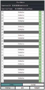
Cassette Mapping: Standard
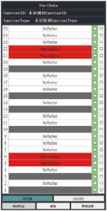
Oblique Insertion
3.High-precision wafer pre-alignment
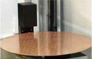
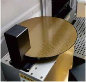
A non—contact optical method is used to locate the center and notch/flat of the wafer.
The fully automated intelligent pre-alignment mechanism achieves accurate and fast positioning of the inspection target. It’s more efficient in operation and more precise in data collection.
Suitable for various wager materials such as Si, SIC, EMC, Glass, etc.
4.Macro Inspection
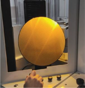
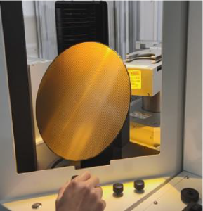
The BAWL-12AS includes a macro inspection are that can perform a 360° rotation for macro inspection of wafer surfaces and backs, making it easy to detect defects and particles on the front, black, and edge sides of the wafer. The wafer can be tilted for observation using the control lever. By rotating and tilting the wager at multiple angles, the entire front, back, and edge of the wafer can be visually inspected. Various light sources, including yellow and green, are available to accommodate different working conditions.
Surface macro inspection
Surface macro inspection
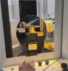
Edge inspection
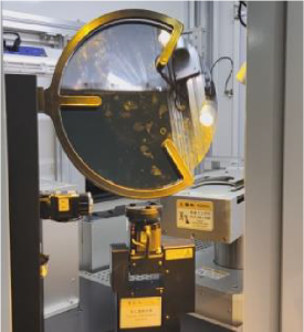
Backside inspection
5.Precision optical micro inspection
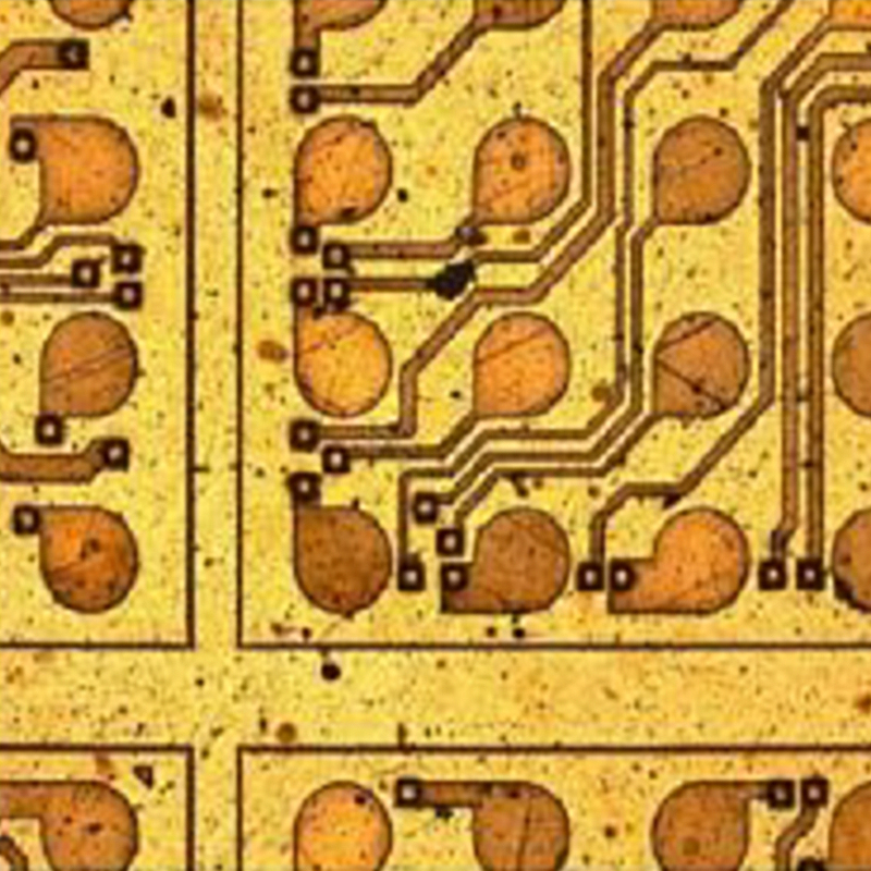
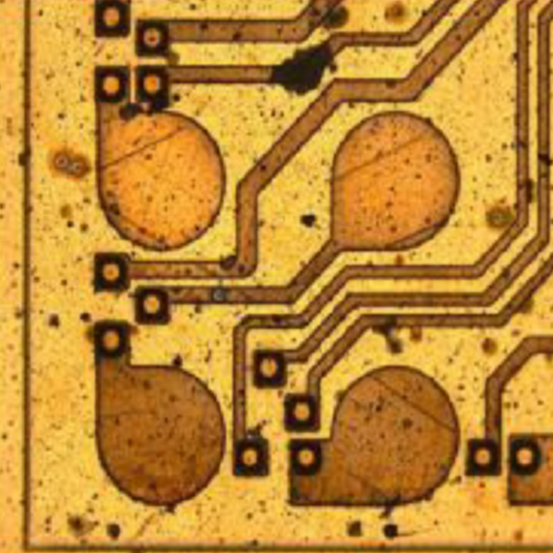
Using a wide-beam imaging system, it supports a world-leading ultra-wide field of view of 25mm, providing a new experience of large-field vision.
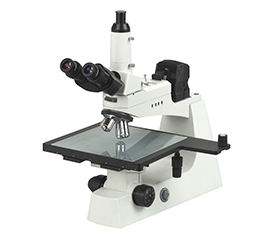
The optical system is equipped with a polarizing system with polarizing and differential interference contrast imaging systems for high contrast, high-resolution micro-imaging.
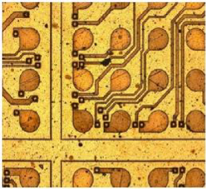
5X Bright Field
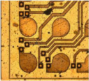
10X Bright Field
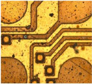
20X Bright Field
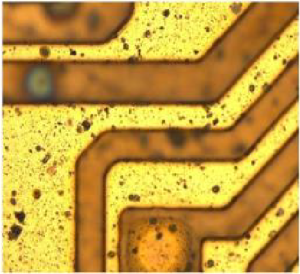
50X Bright Field
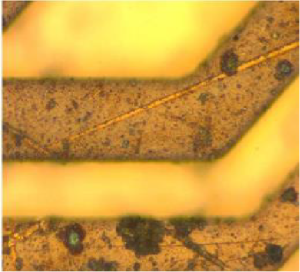
100X Bright Field
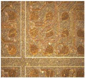
5X Dark Field
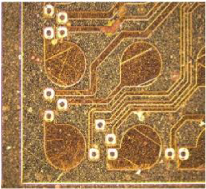
10X Dark Field
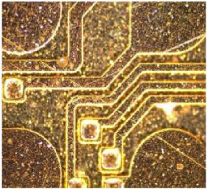
20X Dark Field
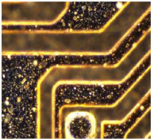
50X Dark Field
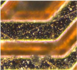
100X Dark Field
6.Precision optical electric components
The equipment’s objective and aperture diaphragm are controlled by an automatic electric control system. The control buttons are in front of the equipment platform, making them easily accessible.
The user-friendly electric design not only avoids frequent manual operations but also make your inspection work more precise and flexible. Controls within reach, helping you improve efficiency.
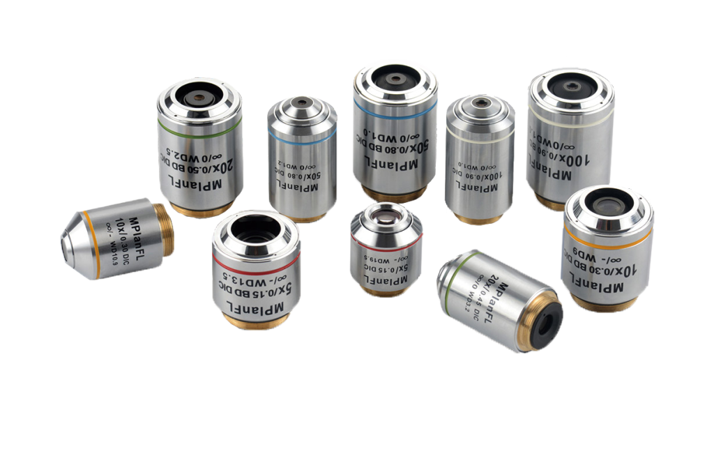
7.Professional APO objective with infinite long working distance
The long working distance BD plan semi-apochromatic metallurgical objectives satisfy observation methods such as bright field, dark field, polarization and DIC. The brightness enhancement of the image in the dark field improves the detection ability of the sample. This series of objective strictly selects high transmittance lenses and advanced coating technology to truly restore the natural color of the sample. The bright and dark field objective is made of special process materials, which greatly reduces weight and contributes to preventing environmental pollution and improving the controllability of objective conversion. The semi-apochromatic design has excellent color correction performance, improving the contrast and clarity of observed images. Long working distance objective lenses are widely used in various testing fields, easily achieving non-destructive testing.
8.Advanced image analysis software
The image processing software, equipped with hardware accessories such as electric platform, electric Z-axis, electric converter, and light source control, supports automatic large image stitching, depth fusion, automatic focusing, 3D measurement, and is compatible with 64-bit Windows systems.
Functions including: auto focus, light source control, electronic control function, measurement module, image library management, depth fusion, particle counting, image stitching, 3D view, 3D measurement.
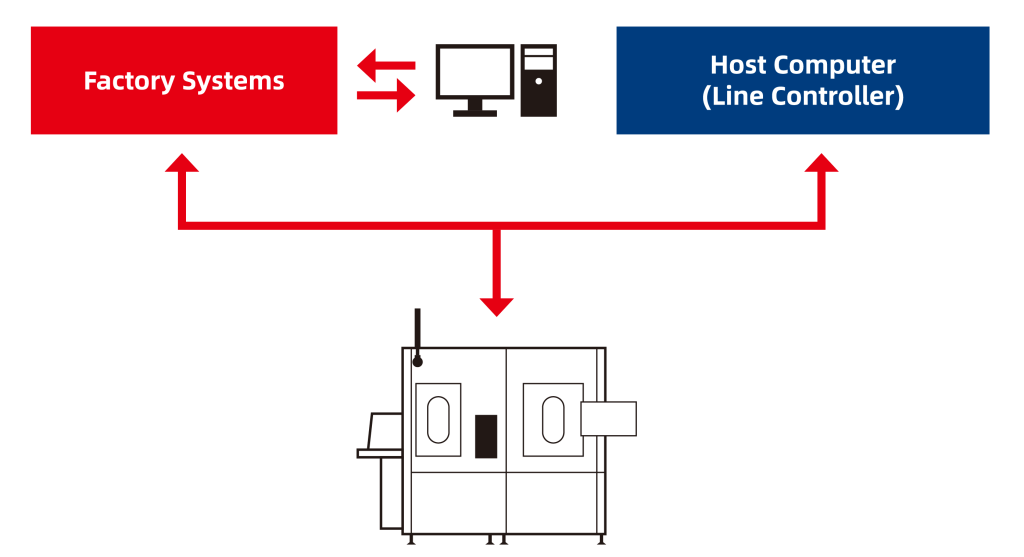
9.Data communication system
The wafer inspection system supports the SECS/GEM semiconductor standard communication protocol, acting as a communication bridge between the equipment and customer MES and other host systems, enabling functions such as work order issuance, material accounting, process recording, and remote control.
The system is equipped with a user-friendly human-machine interface system, making it easy to operate and monitor wafer workstations in real time.
It can recognize various wafer cassette types and is equipped with a high-precision wafer OCR reader. With the unique ID of each wafer, it monitors the entire process data of the wafer. It allows data extraction, modification, and change of the inspection work more efficient and reliable.
The system is compatible with power outage protection devices, allowing the equipment to maintain IPC system operation for 15 minutes in case of power outage, providing enough time for data saving.
10.Reliability
The BAWL-12MS wafer inspection system has high stability and transmission rate. The system uses a safety design compliant with SEMI standards, with built-in UPS uninterruptible power supply, a vacuum holding system, an efficient and stable dual-arm mechanical arm, and various safety interlock functions. It safely and reliably places wafer or warped wafers at various equipment workstation sites.

Specification
|
Item |
Specification |
BAWL-12MS |
BAWL-12AS |
BAWL-12RAS |
|
Wafer Size |
200mm/300mm |
● |
● |
● |
|
Wafer Thickness |
250-1000um/300-1000um |
● |
● |
● |
|
Type of Cassette |
FOUP, FOSB/Smif Pod/Open Cassette |
● |
● |
● |
|
Loadport |
1 Port |
● |
|
|
|
1 Port/2 Ports |
|
● |
● |
|
|
Cassette Mapping |
Standard |
● |
● |
● |
|
FOUP RFID Reader |
Standard |
● |
● |
● |
|
Docking with Crown Block |
Docking with the crown block |
|
○ |
○ |
|
Robot |
Dual arm robotic arm |
● |
● |
● |
|
Pre-Aligner Type |
Non-contact centering |
● |
● |
● |
|
Wafer ID OCR |
Wafer ID OCR |
○ |
○ |
○ |
|
Macro Inspection |
Top surface/Edge/Backside |
● |
● |
● |
|
Macro Inspection Photography |
Macro inspection photography function |
|
○ |
○ |
|
Macro Illumination |
LED, white, yellow and green for optional |
● |
● |
● |
|
Device dimension |
2400mm(W)*1400mm(D)*2350mm(H) (1 port) |
● |
● |
● |
|
2400mm(W)*2050mm(D)*2350mm(H) (2 port) |
|
○ |
○ |
|
|
FFU |
FFU |
● |
● |
● |
|
ESD Static Elimination System |
ESD Static Elimination System |
● |
● |
● |
|
UPS |
Uninterruptible power supply |
○ |
○ |
○ |
|
Power |
Single-phase 220v 50Hz 16A |
● |
● |
|
|
Single-phase 220V 50Hz 32A |
|
|
● |
|
|
CDA |
0.4~0.6Mpa |
● |
● |
● |
|
VAC |
-70KPA~-90KPA |
● |
● |
● |
|
Optical System |
Infinity Color Correction Optical System |
● |
● |
● |
|
Observation method |
Bright field/Dark Field/Polarization/DIC |
● |
● |
● |
|
Eyepiece |
High eyepoint wide field plan eyepiece PL10X/25mm, micrometer and adjustable diopter for optional |
● |
● |
● |
|
Viewing head |
5-35° adjustable, erect image, tilting trinocular head, interpupillary distance: 50-76mm, splitting ratio R:T=100:0 or 0:100 |
● |
● |
● |
|
Objectives |
Long working distance BD plan semi-apochromatic metallurgical objectives 5X/10X/20X/50X/100X |
● |
● |
● |
|
Nosepiece |
Electric sextuple bright and dark field nosepiece, with DIC slot |
● |
● |
● |
|
Focusing |
Manual focusing |
● |
|
|
|
5X objective automatic pre focus |
|
● |
|
|
|
Real time focusing |
|
○ |
● |
|
|
Illumination |
Bright and dark field illumination for reflected, with field diaphragm and electric variable aperture, with switch device of bright and dark field, with slots for filters and polarizing attachment, with 12V/10W LED lamp house |
● |
● |
● |
|
Stage |
12 inches mechanical stage with low position coaxial adjustment in X/Y axis. Wafer holder stage: Φ70mm, 360° rotatable. Observation range: 305mm*305mm. With clutch handle. |
● |
|
|
|
12 inches fully automatic stage, adjustable in X, Y, Z and Φ directions. Wafer holder stage: Φ70mm, 360° rotatable. Observation range: 310mm*310mm, ±5° rotatable on Φ direction, the moving speed on each axis can be switched between high and low speeds. |
|
● |
|
|
|
12 inches fully automatic high precision stage, adjustable in X, Y, Z and Φ directions. Wafer holder stage: Φ70mm, 360° rotatable. Observation range: 310mm*310mm, ±5° rotatable on Φ direction, the moving speed on each axis can be switched between high and low speeds. |
|
|
● |
|
|
Emap System |
Wafer Emap system including visual positioning |
|
○ |
● |
|
Wafer Review System |
Wafer review system |
|
|
● |
|
Import & Export |
Klarf file import and export |
|
|
● |
|
SECS-GEM |
Semiconductor Equipment Communication Standard/Generic Equipment Model |
○ |
○ |
● |
|
Others |
Filters |
○ |
○ |
○ |
|
Polarizer and analyzer |
○ |
○ |
○ |
|
|
DIC kit |
○ |
○ |
○ |
|
|
C-mount adapter |
○ |
○ |
○ |
|
|
Camera |
○ |
○ |
○ |
|
|
Professional software for wafer inspection |
○ |
○ |
○ |
Note: ● Standard Outfit, ○ Optional


