


BSEM-320B Tungsten Filament Scanning Electron Microscope
Introduction
BSEM-320B is a high-performance tungsten filament scanning electron microscope. It has excellent imaging quality capabilities in both high and low vacuum modes. It also has a large depth of field with a user-friendly interface to enable users to characterize specimens and explore the world of microscopic imaging and analysis.
Details
Overview
Packaging & Delivery
Packaging Details:Strong Carton with Polyfoam Protection
Port:Beijing
Lead Time:Within 2-4 Weeks after Receiving Payment
Introduction
BSEM-320B is a high-performance tungsten filament scanning electron microscope. It has excellent imaging quality capabilities in both high and low vacuum modes. It also has a large depth of field with a user-friendly interface to enable users to characterize specimens and explore the world of microscopic imaging and analysis.
Features
1. Low Voltage
Carbon material specimens with shallow penetration depth at low voltage. The true topography of the specimen surface can be obtained with rich details.
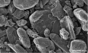 Low Voltage-Carbon
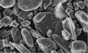 High Voltage-Carbon
The electron beam irradiation damage of the hair specimen is reduced at low voltage while the charge effect is eliminated.
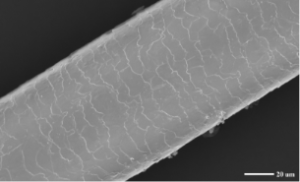 Low Voltage-Carbon
 High Voltage-Carbon
2. Expandability
BSEM-320 has a large specimen chamber with an extensive interface: SEM SE\BSE\EDS\EDX\EBSD, etc.
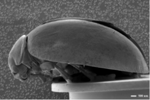
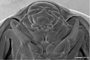
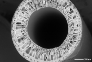
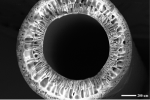
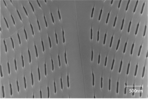
3. Large Field of View
Biological specimens, using a large field of view observation, can easily obtain the overall morphology details of a ladybug’s head, demonstrating cross-scale imaging ability.
4. Optical Navigation
Quickly locates targeted Region of Interest (ROI). Click where you want to go and see with easy navigation. An in-chamber camera is standard and can take HD photos to help locate specimens quickly.
5. Quick Gesture Navigation
Quick navigation by double-clicking to move, middle mouse button to drag, and frame to zoom.
Exp: Frame Zoom – to get a large view of the specimen with low magnification navigation, you can quickly frame the specimen area you are interested in, image zooms in automatically to improve efficiency.

6. Intelligence Assisted Image Astigmatism Correction
Visually display astigmatism within the entire field of view, and quickly adjust to correct by mouse clicking.

7. Auto Focus
One-button focus for fast imaging.
8. Automatic Stigmator
One-click astigmatism deduction to improve work efficiency.
9. Auto Brightness & Contrast
One-click auto brightness & contrast to tune appropriate images’ grayscale.
10. Mixed Imaging (SE + BSE)
Observe the specimen compositional and surface topographic information in one image. The software supports one-click switching between SE and BSE for mixed imaging. Both morphological and compositional information of the specimen can be observed at the same time.
11. Fast Image Rotation Adjustment
Drag a line and release to rotate the image right on the spot.
12. Stage Anti-collision
A multi-way anti-collision solution:
Manually input specimen height: precisely control the distance between the specimen surface and the objective lens.
Image recognition and motion capture: monitor the real-time stage movement.
Hardware: shut down the stage motor at the moment of collision. (BSEM-320A requires this function as an optional feature)
13. Dual Anode (Tetrode)
Dual anode emission system design provides excellent resolution under low landing energy.
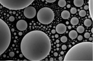
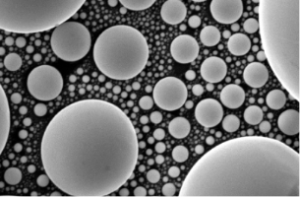
14. Low Vacuum Mode
Provides specimen surface morphology information in low vacuum, switchable vacuum state with one click.
Filtered fiber tube materials are poorly conductive and charge significantly in high vacuum. In the low vacuum, direct observation of non-conductive specimens can be achieved without coating.
 Low Vacuum
 High Vacuum
Application
1. Semiconductors and Electronic Component
 Ordinary Chips-1 / 10kV / ETD
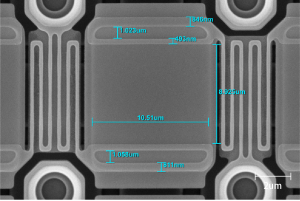 Ordinary Chips-2 / 10kV / ETD
2. Batteries and New Energy
 Cathode-Carbon / 5kV / ETD
 Anode-Lithium Cobaltates / 15kV / ETD
 Solar Battery-1 / 5kV / ETD
 Solar Battery-2 / 10kV / ETD
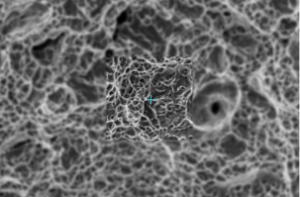
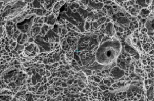
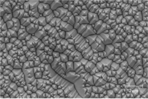
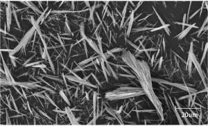
3. Polymer Materials
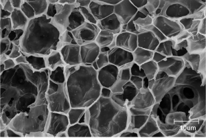
Polymer Foam / 15kV
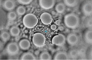
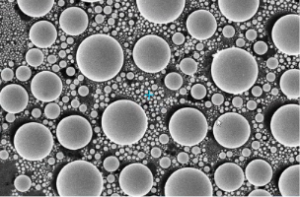
4. Chemicals
MOF-Material / 15kV / ETD
5. ETD Metal
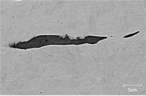
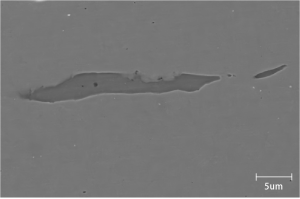
 Stainless Steel-Brass Weldments / 15kV / BSED
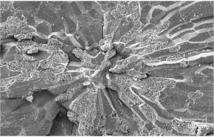
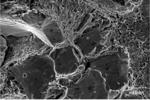 Alloy Fracture Brittleness + Toughness / 20kV / ETD
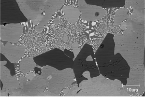
 Iron and Steel Inclusions / 15kV / BSED
 Iron and Steel Inclusions / 15kV / ETD
6. Biological
 Diatom / 10kV / ETD
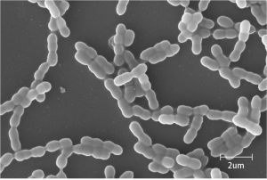 Staphylococcus Gallinarum / 15kV / ETD
7. Food
 Rice / 10kV / ETD
 Waxy Rice Starch Granules / 10kV / ETD
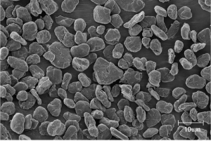
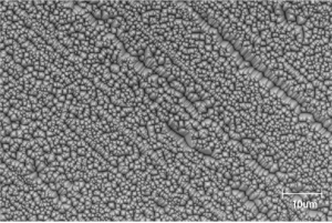
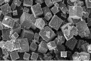
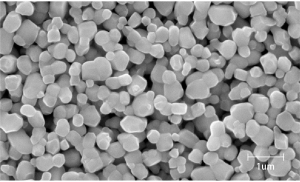
8. Fundamental Research
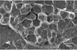
 Powder – Magnesium Sulfate / 15kV / ETD
 Powder Barium Titanate / 25kV / ETD
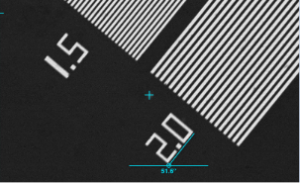
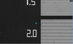
Specification
|
Item |
Specification |
BSEM-320A |
BSEM-320B |
||
|
Electron Optical System |
Pre-aligned Medium-sized Hairpin-type Tungsten Filament |
● |
● |
||
|
Resolution |
High Vacuum: 3nm@30kV (SE), 4nm@30kV (BSE), 8nm@3kV (SE) |
● |
● |
||
|
Low Vacuum: 3nm@30kV (SE) |
○ |
○ |
|||
|
Magnification:1-300,000x (film), 1-1000,000x (screen) |
● |
● |
|||
|
Accelerating voltage: 0.2kV-30kV |
● |
● |
|||
|
Imaging System |
Everhart-Thornley Detector (ETD) |
● |
● |
||
|
Backscattered electron detector (EBSD) |
○ |
○ |
|||
|
Low vacuum secondary electron detector |
○ |
○ |
|||
|
Energy spectrometer EDS |
○ |
○ |
|||
|
BSE |
○ |
○ |
|||
|
Vacuum System |
High vacuum: better than 5*10-4Pa |
● |
● |
||
|
Low vacuum: 5-1000Pa |
○ |
○ |
|||
|
Control Mode: Fully automatic. Turbo molecular pump:>240L/s. Mechanical pump: 200L/min (50Hz) |
● |
● |
|||
|
Specimen Chamber |
Camera |
Optical Navigation |
● |
● |
|
|
Monitoring in the Specimen Chamber |
● |
● |
|||
|
Specimen Table |
Three Axis Automatic |
● |
|
||
|
Five Axis Automatic |
|
● |
|||
|
Stage Range |
X: 120mm. Y: 115mm. Z: 50mm. |
● |
|
||
|
X: 120mm. Y: 115mm. Z: 50mm. R: 360° T: -10°- +90° |
|
● |
|||
|
Software |
Windows. Optical Navigation, Gesture Quick Navigation. Auto Brightness & Contrast, Auto Focus, Automatic Stigmator and Intelligence Assisted Image Astigmatism Correction |
● |
● |
||
|
Large-FOV Image Stitching |
○ |
○ |
|||
|
Installation Requirements |
Space: L≥ 3000 mm, W ≥ 4000 mm, H ≥ 2300 mm Temperature: 20°C (68°F) ~ 25°C (77°F) Humidity: ≤ 50 % Power Supply: AC 220 V(±10 %), 50Hz, 2kVA |
● |
● |
||
Note: ● Standard Outfit, ○ Optional
Accessories
The scanning electron microscope (SEM) is used not only for the observation of surface morphology but also for the analysis of the composition of micro-regions on the specimen surface.
BSEM-320 has a large specimen chamber with an extensive interface. In addition to supporting conventional Everhart–Thornley detector (ETD), Backscattered-Electron detector (BSE), and Energy-dispersive X-ray spectroscopy (EDS/EDX), various interfaces such as Electron Backscatter Diffraction Pattern (EBSD) and Cathodoluminescence (CL) are also reserved.
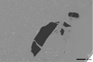
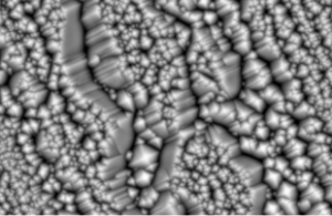
1. Backscattered-Electron Detector (BSE)
Comparison of secondary electron imaging and backscattered electron imaging
In the backscattered electron imaging mode, the charge effect is significantly suppressed and more information on the composition of the specimen surface can be observed.
Plating Specimens:

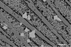
Tungsten Steel Alloy Specimens:
2. Four-quadrants Backscattered Electron Detector – Multi-channel Imaging
The detector has a compact design and high sensitivity. With the 4-quadrants design, it is possible to obtain topographic images in different directions as well as composition distribution images without tilting the specimen.
 Component Images
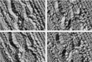 Four One-channel Images
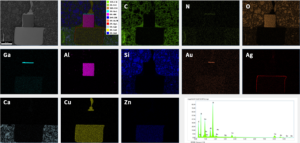
3. Energy Spectrum
LED small bead energy spectrum analysis results.
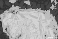
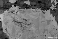
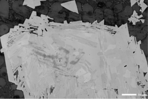
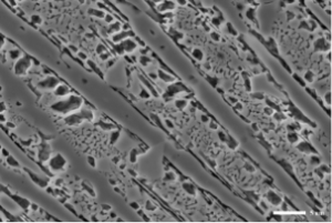
4. Electron Backscatter Diffraction Pattern (EBSD)
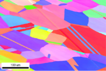
The tungsten filament electron microscope with a large beam current fully meets the testing requirements of high-resolution EBSD and can analyze polycrystalline materials such as metals, ceramics, and minerals for crystal orientation and grain size analysis.
The figure shows the EBSD grain map of Ni metal specimen, which can identify grain size and orientation, determine grain boundaries and twins, and make accurate assessments of material organization and structure.