
What is Scanning Electron Microscope?
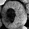
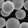
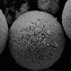
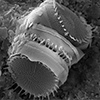
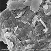
A scanning electron microscope (SEM) uses an electron gun to emit a focused beam of high-energy electrons. When the electron beam strikes the surface of a sample, it excites a variety of signals, including secondary electrons, backscattered electrons, absorbed electrons, Auger electrons, cathodoluminescence, and characteristic X-rays. By detecting, amplifying, and imaging these signals, SEM allows for the detailed observation of surface morphology and analysis of the sample’s structural and compositional characteristics. Among these signals, secondary electrons, backscattered electrons, and characteristic X-rays are primarily used for surface feature analysis in SEM.
At BestScope, we specialize in delivering advanced solutions in scanning electron microscopy. With a strong focus on innovation and quality, we develop and manufacture a full range of high-performance SEM systems, including tungsten filament SEMs, field emission gun SEMs, and sputter coaters. Our products are widely trusted in cutting-edge research and industrial applications across semiconductors, new energy, and materials science. We are committed to helping you achieve precise, reliable imaging results for even the most demanding tasks.
Tungsten Filament Scanning Electron Microscope
Designed for performance and versatility, our systems combine advanced electron-optical technology, wide sample adaptability, low vacuum compatibility, user-friendly operation, and customizable configurations.

Resolution: 3nm@30KV (SE), 8nm@3KV (SE), 4nm@30KV (BSE).
Resolution: 3nm@30kV (SE) High Vacuum, 4nm@30KV (BSE) High Vacuum, Low Vacuum.
Field Emission Scanning Electron Microscope
Equipped with an excellent electron-optical system and outstanding imaging performance, our microscopes offer easy operation and versatile application expandability to meet a wide range of research and industrial needs.

Positioned as an affordable Schottky thermal field emission SEM, BSEM-801 offers excellent expandability and cost-effectiveness, making it ideal for analytical and processing needs across industries such as metallurgy and materials science.

With a newly designed electron-optical system featuring column acceleration technology and a low-aberration conical objective lens, BSEM-810 is optimized for high-quality imaging and user experience at low accelerating voltages. It is well-suited for observation needs in fields such as semiconductors and life sciences.
Application
Utilize scanning electron microscopy to reveal the microstructure of metal materials in depth, supporting performance optimization and advanced material development.
Scanning electron microscopy enables high-resolution imaging of microstructures, structural analysis, defect detection, compositional analysis, and failure analysis in semiconductor materials.
Scanning electron microscopy is widely used in the new energy sector for observing the microstructure, analyzing the composition, characterizing the structure, and conducting failure analysis of materials such as lithium-ion batteries.
Scanning electron microscopy enables high-resolution observation of the morphology and structure of cells, tissues, and microorganisms, providing valuable data support for research in cytology, histology, and pathogen studies.
Scanning electron microscopy is used for micro-area morphology observation, structural analysis, and high-precision compositional analysis of materials such as minerals, rocks, and construction materials.

Scanning electron microscopy is used to examine and analyze trace evidence such as fibers, hair, particles, and paint, providing critical support for criminal investigations.
Using Scanning Electron Microscopy to observe and analyze the microstructure, morphology, and composition of functional materials at high resolution, in order to assist in the development and performance optimization of new materials.

Scanning electron microscopy is used to perform high-resolution microstructure observation, structure analysis, phase separation structure characterization, and material failure analysis of the polymer materials.
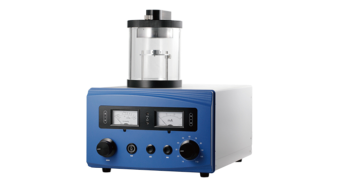
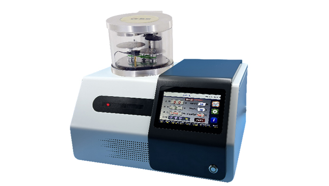
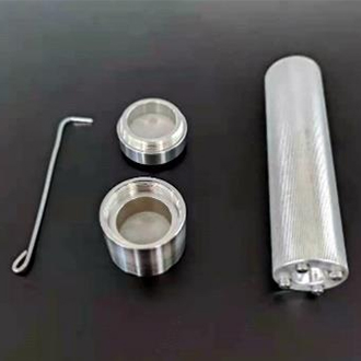
BISC-12 Mini Ion Sputter Coater
BISC-12 is mainly used for coating conductive films on SEM samples, it is simple to operate, cost-effective, and durable. It is an essential tool for sample preparation in conjunction with small to medium-sized scanning electron microscopes.
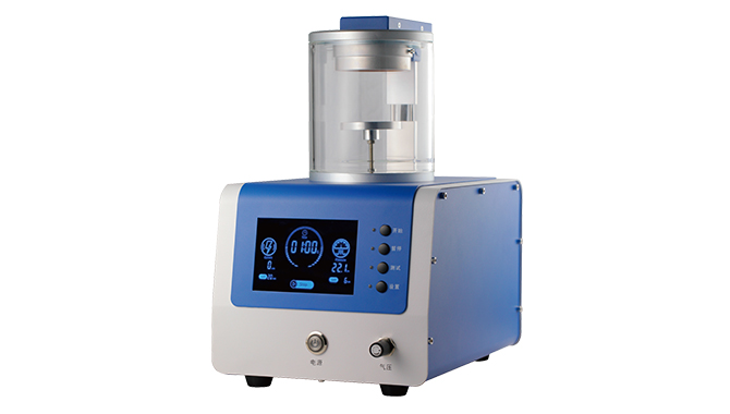
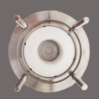
BISC-16 Magnetron Ion Sputter Coater
BISC-16 is primarily designed for coating non-conductive samples in SEM imaging, this system is especially suitable for temperature-sensitive specimens, ensuring no thermal damage. It is also applicable for electrode and metal film deposition, offering a wider range of uses.
BESC-50T High Vacuum Evaporation and Sputtering Coater
One-click switch between sputtering and evaporation modes, easy operation, fast start-up, clean coating, and ideal for high-resolution observation of various samples.
- Gallery
- Feature
- Specification

- LCDtouch screen.
- Not suit able for dust free room.
- Manual,auto and loop mode.
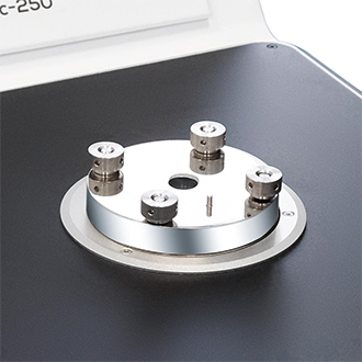
- Suitable for SEM, TEM, MEMSetc. sample preparation.
- Built-in pressure control,automatically control system pressure and maintain stability of pressure.
- Multiple default processing program, customized available.
- Observation window with light for observing the state of sample.
- Built-in filter system, protect sample and valve.
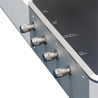
- External 5μm filter, remove water,oil and particle.
- Micro metering valve controls the flow of LCO2with scale.
- Operating parameter repeatable setting available, make sure the repeatability of result.
|
Specification |
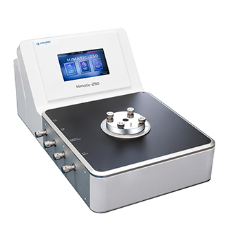
Himatic-250 |
|
Control |
LCD touch screen control Fully automatically control |
|
Chamber Size |
2.5″ (Inner diameter) *1.25″ (Depth) |
|
Chamber Volume |
100 ml |
|
Dimension |
31.5cm (H)*39.3cm (W)*58.2cm (L) |
|
Temperature Pressure Range |
– 30°C ~ 60°C, 0 ~2000 psi |
|
Configuration |
Flexible high pressure LCO2 pipeline, 2m External LCO2 filter unit (remove particle over 0.5 μm) Antistatic and anti-freezing discharge pipeline Sample chamber sealing ring*2 Chamber bulb*2 Installation kit Wrench Touch screen pen Flowmeter Operation Manual |