


BSEM-500X Ultra-high Resolution Field Emission Scanning Electron Microscope
Introduction
BSEM-500X is an ultra-high resolution Field Emission Scanning Electron Microscope with breakthrough resolution of 0.6 nm@15 kV and 1.0 nm@1 kV. Benefited from the upgraded column engineering process, “Super Tunnel” technology, and high-resolution objective lens design, BSEM-500X is able to achieve further improvements in low-voltage imaging resolution.
Details
Overview
Packaging & Delivery
Packaging Details:Strong Carton with Polyfoam Protection
Port:Beijing
Lead Time:Within 2-4 Weeks after Receiving Payment
Introduction
BSEM-500X is an ultra-high resolution Field Emission Scanning Electron Microscope with breakthrough resolution of 0.6 nm@15 kV and 1.0 nm@1 kV. Benefited from the upgraded column engineering process, “Super Tunnel” technology, and high-resolution objective lens design, BSEM-500X is able to achieve further improvements in low-voltage imaging resolution. The specimen chamber ports extend to a number of 16, and the specimen exchange load-lock supports up to 8-inch wafer size (maximum diameter 208 mm), which greatly expand the coverage of applications. The advanced scanning modes and enhanced automated functions bring stronger performance and an even more optimized experience.
Features
1. Ultra-high resolution
Ultra-high resolution imaging with breakthrough 0.6nm@15kV and 1.0nm@1kV.
2. Super Tunnel Technology
Dual deceleration technology combining specimen stage tandem deceleration and “Super Tunnel” technology, ready to challenge extreme imaging conditions.
3. Mechanical Eucentric Specimen Stage
High-precision mechanical eucentric specimen stage, ultra-stable vibration-damping design, also available with integral enclosure option, greatly minimized the environmental interference that could impact the resolution.
4. Specimen Exchange Loadlock
Specimen exchange loadlock with up to 8″ wafer size (Maximum 208 mm in diameter), meets the needs of semiconductor and research applications.
5. Focused Ion Beam Column
The focused ion beam column which outputs a highly stable, high-quality ion beam, suit able for high-quality nano-fabrication and TEM specimen preparation.
Application
 Mesoporous Silica 1kV (Dul-Dec)/Inlens
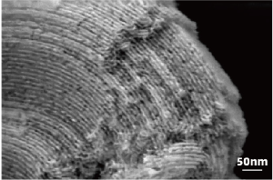
 Anodized Aluminum Plate 10kV/Inlens
 IC Clip 5kV/BSED-COMP
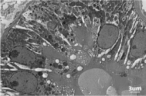 Kidney Sections 5kV/BSED-COMP
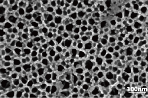
 Nickel Foam 2kV/ETD-SE
 Sapphire Substrate 5kV/ETD-SE
 Gold Particles 1kV/Inlens
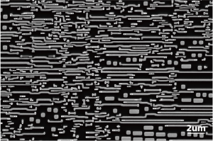
 Photoresist 2kV/ETD-SE
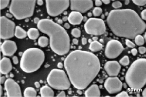
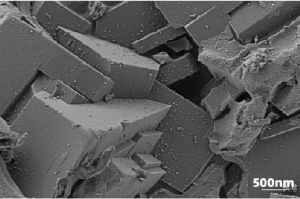
 Magnetic Powder 10kV/Inlens
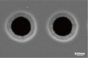
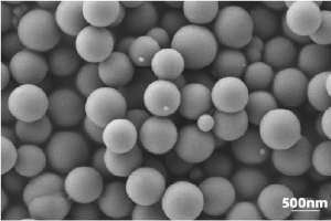 Silicon Dioxide Spheres 3kV/ETD-SE
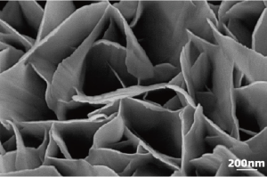
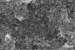
 Catalyst 1kV/ETD-SE
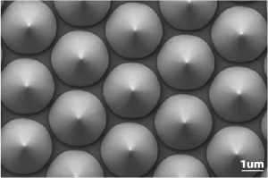
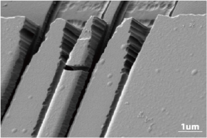 Waveguide 1kV/ETD-SE
Specification
|
Item |
Specification |
BSEM-500X |
|
|
Electron Optical System |
Schottky Field Emission Electron Gun |
● |
|
|
Resolution: 0.6nm@15kV (SE), 1.0nm@1.0kV (SE) |
● |
||
|
Magnification: 1-2,500,000x |
● |
||
|
Accelerating voltage: 20V-30kV |
● |
||
|
Detector and Extension |
In lens Detector |
● |
|
|
Everhart-Thornley Detector (ETD) |
● |
||
|
Retractable Back-Scattered Electron Detector (BSED) |
○ |
||
|
Retractable Scanning Transmission Electron Microscopy Detector (STEM) |
○ |
||
|
Energy Dispersive Spectrometer (EDS) |
○ |
||
|
Electron Backscatter Diffraction Pattern (EBSD) |
○ |
||
|
Specimen Exchange Loadlock (4″ & 8″ optional) |
○ |
||
|
Trackball & Knob Control Panel |
○ |
||
|
Specimen Stage Tandem Deceleration |
○ |
||
|
Magnetic Field & Acoustic Noise Enclosure System (SEMI Certified) |
○ |
||
|
Specimen Chamber |
Vacuum system: Fully Automated Control |
● |
|
|
Camera |
Dual Cameras |
● |
|
|
Optical navigation |
○ |
||
|
Chamber monitor |
○ |
||
|
5-Axis Mechanical EU centric Specimen Stage |
● |
||
|
Stage Range: X: 110mm. Y: 110mm. Z: 65mm. R: 360° T: -10°- +70° |
● |
||
|
Software |
Windows. Nav-Cam, Gesture Quick Navigation. Auto Brightness Contrast, Auto Focus, Auto Stigmator. |
● |
|
Note: ● Standard Outfit, ○ Optional